Watch it print.
A 3D printer builds this chip by hardening one thin slice of liquid plastic at a time. This one takes 1,150 slices, each a hundredth of a millimetre thick. Scroll to watch it build. These are not drawings — each picture is a real slice through the design.
The block accumulates
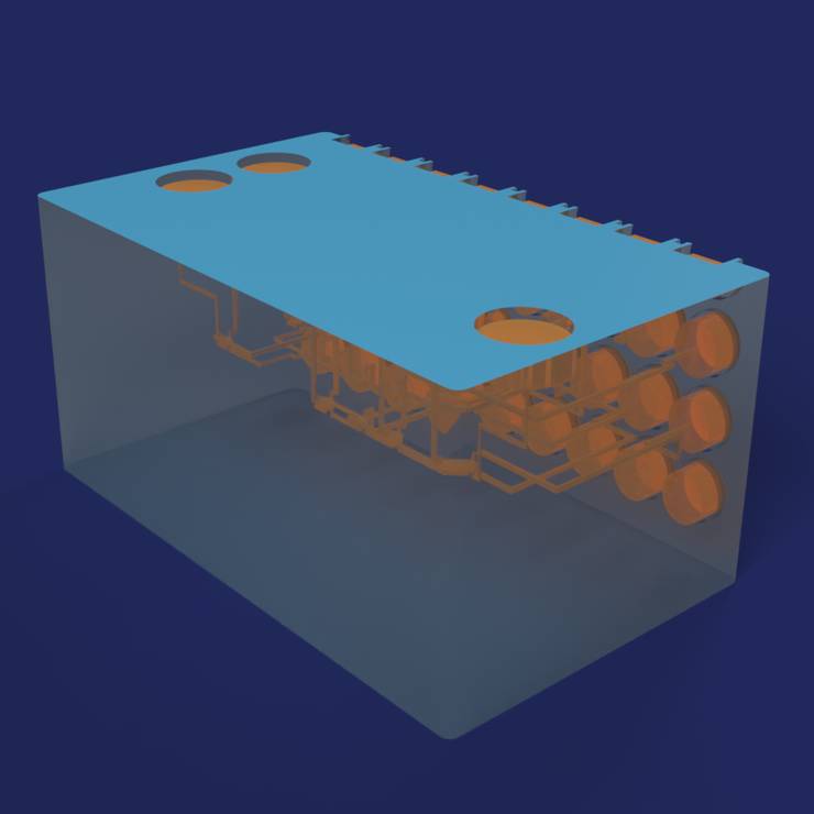
The printer cures one full cross-section of resin, drops ten microns, and cures the next. Nothing is carved and nothing is joined — the part grows upward out of the vat. Cyan is the cross-section being written at this instant.
What is already sealed inside
Cured resin is translucent, so the block is drawn see-through here and the finished interior shows through it. Amber marks void — channels and chambers already roofed over below the build plane. Nothing was drilled and nothing was bonded: the printer simply never cured resin there. That liquid resin still has to be cleared out after printing, and the lab reports prints where it could not be (Hardware and process, section 6).
The pump and the mixer
The widest cross-sections belong to the nine pneumatically actuated chambers that give the chip its name. Each carries a pressure line and a purge line — eighteen pneumatic ports in all.
One part, no assembly
Roof closed, only the ports still open. Pump, mixer, nine chambers and all twenty-six routed nets — designed to leave the printer as a single monolithic block, 19.46 × 12.05 × 11.50 mm, with no bonding step.
Technical details
A CAD design for experimental printing. The geometry is watertight, DRC-clean and topologically checked in CAD.
Geometry credit: Nordin Group, BYU, with the State of Utah Center of Excellence for Biomedical Microfluidics, University of Utah. The design shown on this page is the Nordin Group's, BYU, and its images here are not under this site's MIT licence; for their terms, ask the Nordin Group. · Back to the library